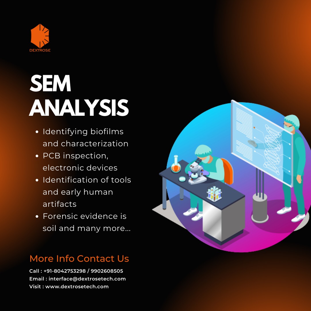
SEM is a powerful tool that allows researchers to study the surface features of specimens at a micro- to nanometer scale. It works by using focused beams of electrons to render high-resolution, three-dimensional images. These images provide information on the topography, morphology, and composition of the sample. SEMs are used for research, quality control, and failure analysis in materials science. They are also used in modern semiconductor inspection and the analysis of cosmetic components that are very tiny in size. In summary, SEM is an essential tool for research in various scientific disciplines such as materials science, biology, geology, and nanotechnology. 🌟 For more details, visit dextrosetech.com. You can also us at +91-8042753298.

This is your website preview.
Currently it only shows your basic business info. Start adding relevant business details such as description, images and products or services to gain your customers attention by using Boost 360 android app / iOS App / web portal.
2024-03-11T05:30:38
SEM is a powerful tool that allows researchers to study the surface features of specimens at a micro- to nanometer scale. It works by using focused beams of electrons to render high-resolution, three-dimensional images. These images provide information on the topography, morphology, and composition of the sample. SEMs are used for research, quality control, and failure analysis in materials science. They are also used in modern semiconductor inspection and the analysis of cosmetic components that are very tiny in size. In summary, SEM is an essential tool for research in various scientific disciplines such as materials science, biology, geology, and nanotechnology. 🌟 For more details, visit dextrosetech.com. You can also us at +91-8042753298.
2024-03-11T05:30:38
Share it on


Keywords
- size
- SEMs
- sample
- geology
- biology
- summary
- details
- specimens
- micro- to
- electrons
- morphology
- topography
- composition
- information
- researchers
- dextrosetech
- focused beams
- powerful tool
- essential tool
- nanotechnology
- quality control
- nanometer scale
- surface features
- failure analysis
- materials science
- cosmetic components
- various scientific disciplines
- modern semiconductor inspection
- high-resolution, three-dimensional images
Submit Your Enquiry