

Small defects can have a major impact on semiconductor performance.
Microcracks, contamination, coating irregularities and interface defects can hold valuable clues to material and device failures.
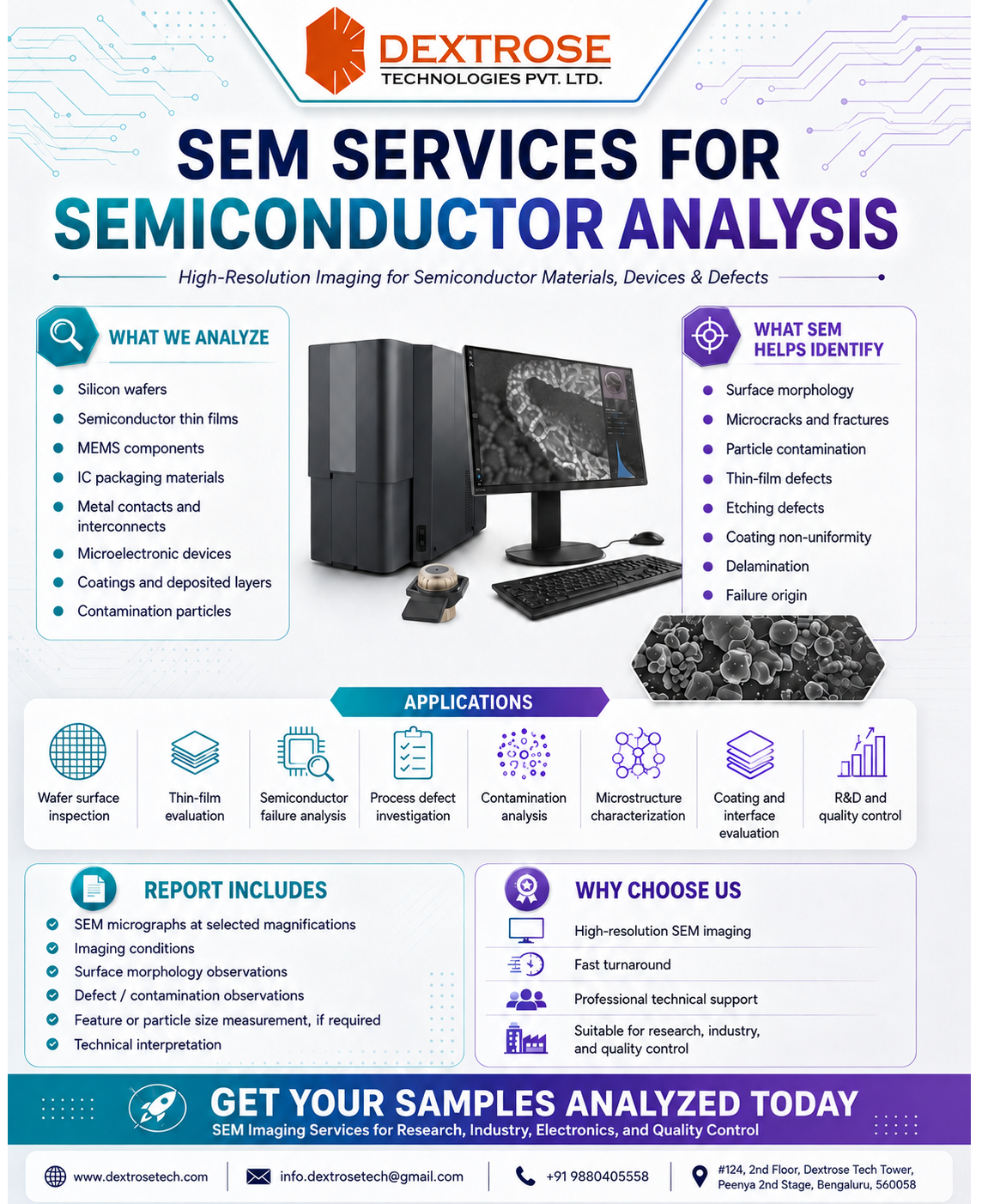
At Dextrose Technologies, our SEM Services for Semiconductor Analysis help research and industry teams examine surface features and investigate defects.
🔬 Materials and components we analyse:
Silicon wafers and semiconductor thin films
MEMS components and microelectronic devices
IC packaging materials
Metal contacts and interconnects
Coatings, deposited layers and contamination particles
Our SEM analysis supports wafer surface inspection, thin-film evaluation, contamination investigations, microstructure characterisation and failure analysis.
Reports include SEM micrographs at selected magnifications, imaging conditions, morphology and defect observations, technical interpretation, and feature or particle size measurements where required.
Share your sample details and the issue you want to investigate. Our team will help define the analysis scope and provide a quote.
📞 +91 9880405558
📩 info.dextrosetech@gmail.com
🌐 www.dextrosetech.com